


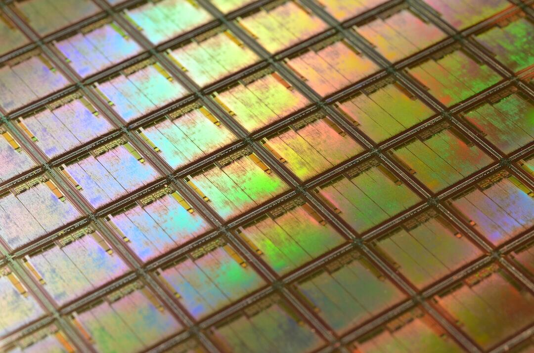
Silicon wafers are used to build most small electronic devices. They serve as the base for creating layers and patterns that power chips and sensors. These wafers allow manufacturers to make parts that are smaller and more accurate. They help improve how devices perform and extend their lifespan.
Many industries use them to produce faster and more efficient systems. Each wafer goes through controlled steps to ensure high-quality results.
Learn how patterned silicon wafers are driving precision and progress in microfabrication below.
Table of Contents
Role of Patterned Wafers in Microfabrication
Patterned wafers are used to form structures at the smallest levels of device production. Each wafer passes through steps like oxidation, lithography, and etching. These steps create the detailed patterns that guide electrical flow in circuits. The design accuracy determines how well a chip performs.
A small error can affect how the entire system works. Manufacturers can repeat these patterns across many wafers with the same results. This makes production faster and more reliable. The role of precise patterning is central to every microfabrication process.
Advancements in Patterned Silicon Wafers
Patterned silicon wafers are key to creating high-performance micro devices. Each wafer holds detailed patterns that guide how circuits and layers form. These patterns make it possible to build smaller, faster, and more reliable components.
The process uses advanced methods like lithography and etching to create exact designs. This helps improve how signals move and how energy is used inside chips.
Consistent patterning also reduces errors and improves product life. As technology evolves, these wafers continue to shape the direction of modern microfabrication. Their precision supports the development of the next generation of electronics.
Advancements in Photolithography Techniques
Photolithography is the method used to print patterns on silicon wafers. It uses light to transfer images onto the wafer surface. The technique has improved through the use of shorter light wavelengths. These allow smaller and sharper patterns to be created.
The process also involves advanced alignment systems that ensure each new layer matches the one before it. This prevents overlap or misplacement in circuits. Modern methods like ultraviolet light printing make even finer details possible. This advancement supports the production of faster and smaller devices.
Etching Methods for Greater Accuracy
Etching removes unwanted parts of the wafer surface to form exact shapes. Wet etching uses liquid chemicals while dry etching uses gas or plasma. Dry etching gives more control and produces cleaner lines. Both are important for keeping pattern dimensions accurate.
The choice depends on the required shape and the material being used. These processes define how deep or wide each pattern will be. Proper etching keeps each circuit uniform across the wafer. It ensures better performance in every device made from it.
Importance of Cleanroom Environments
Wafers must be made in clean environments to prevent contamination. A single particle can cause damage that affects the entire wafer. Cleanrooms use special filters that remove dust and other contaminants from the air. Workers wear protective suits to avoid releasing particles.
The temperature and humidity are controlled to keep the process stable. Every production stage happens inside these controlled rooms. This helps keep wafer quality consistent and reduces waste. Clean environments ensure each patterned wafer meets strict quality standards.
Thin Film Deposition for Layer Precision
Thin film deposition builds the layers needed for electronic function. Each film acts as a conductor, insulator, or semiconductor. The thickness of each layer must be exact for the device to work properly.
Common methods include chemical vapor deposition and physical vapor deposition. These methods apply material evenly on the wafer surface. They also improve bonding between layers for stability.
Thin film control helps reduce performance problems in circuits. Reliable layering supports long-term efficiency in microfabrication.
Optical Inspection and Quality Assurance
Inspection is done to find and fix any surface issues before mass production. Optical tools and microscopes scan each wafer for defects. The systems can detect tiny scratches or pattern misalignments. Early detection prevents costly production errors.
Inspection also checks if all layers are aligned correctly. This process ensures that electrical paths follow the right design. Consistent testing maintains reliability and helps meet production standards. Quality assurance keeps the final products stable and high-performing.
Applications in Sensor Manufacturing
Patterned wafers are used to produce sensors that measure pressure, heat, or motion. These sensors are found in many devices used every day. The precision of the wafer patterns helps sensors collect data accurately. High pattern quality allows better calibration and faster signal response.
As sensors get smaller, wafer-level designs help make them stronger and more reliable. The materials also allow sensors to handle tough environments. Consistent wafer quality improves how sensors work in various fields. Reliable sensor production depends on precise microfabrication.
Enhancing Semiconductor Chip Performance
Semiconductor chips perform better when built on precise wafers. Proper patterning reduces resistance and improves signal flow. This makes chips faster and more energy-efficient. Uniform wafer surfaces help manage heat better during operation.
Reliable patterning also supports longer chip life. Manufacturers use these wafers to keep designs consistent in large-scale production. Each patterned wafer must meet exact electrical and mechanical standards. This precision ensures the steady improvement of chip technology.
Role in MEMS Device Fabrication
MEMS devices depend on patterned wafers to combine mechanical and electronic functions. These devices include sensors, switches, and actuators. Each part must fit and move correctly within a very small space.
The wafer provides the structure that keeps all components stable. It also ensures smooth electrical connections between moving parts. MEMS are used in vehicles, medical tools, and communication systems.
Their accuracy depends on how well the wafer is patterned. Microfabrication continues to refine this process to achieve higher reliability.
Integration with Nanotechnology
The combination of microfabrication and nanotechnology has led to smaller and smarter devices. Patterned wafers make this integration possible by providing stable platforms for nanoscale designs.
Nanostructures improve how materials conduct electricity or light. This creates faster and more efficient devices. The precision of the wafer surface supports controlled pattern growth. Such designs are used in medical devices, optics, and advanced computing.
Patterned Silicon Wafers Helps With Precision Microfabrication
Patterned silicon wafers are the main tools behind progress in microfabrication. They help create smaller, faster, and more accurate devices. Every stage of production relies on their precision and consistency.
As demand for better technology grows, improvements in wafer processes will continue. Their importance in electronics and sensor development remains strong.
More accurate designs mean more reliable results. The drive for precision will keep shaping the future of advanced manufacturing.
For other topics, check our blog!